We are going to implement 8 chips in this project.
The Chips to implement
1-Bit Register Chip
Tip: It can be built from a DFF and a multiplexor.
16-Bit Register
Tip: A little bit different wiring from the last one.
8-Register Chip
This is the first RAM device consisting of 8 registers. Here is its API:
1 | CHIP RAM8 { |
Tips:
- We need to feed the
invalue to all the 8 registers simultaneously. - Then use the Mux or DeMux chips to select the one to operate.
RAM64, RAM512, RAM4K,RAM16K
Tips:
As we started the last RAM8, we can stack the small RAM chip to larger ones, grouping them layer by layer.
Think about the address input as consisting of 2 fields: one to select the RAM, the other to select the register.
Program Counter
Tip: It can be built from a register, an incrementor and other taught gates.
Some Questions
Q. Why there are 2 folders a/ and b/ in Project 3 directory?
A. The larger RAMs, like RAM16K, are built from smaller ones down to the Bit Register, so it will involves a huge recursion. This will be too much for a humble simulator to handle. Therefore, we are supposed to use the built-in Java implementations, which makes it faster and smoother.
Q. We take the Flip Flop as a black box in this course. How is it implemented in real?
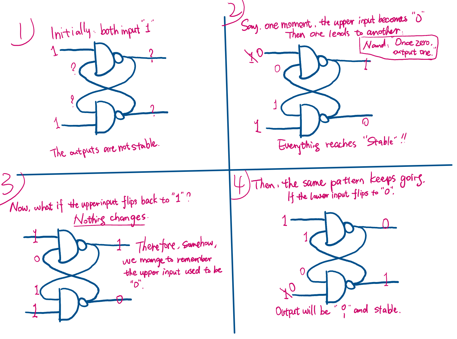
A. The core is 2 NAND Gates connected in a loop. A change in a moment can decide the output in the future.

Above shows how gate maintains “memory”. Of course the outer layer is necessary for the DFF functionality.
While Doing It
- HDL is a description language not a programming language. It is OK to input a new pin name, which appears in the line below, to implement the circle between gates.