Memory Units (Unit 3.3)
Given the 1-bit register we learned in the last post, we can build more things!
The basic memory element: Register
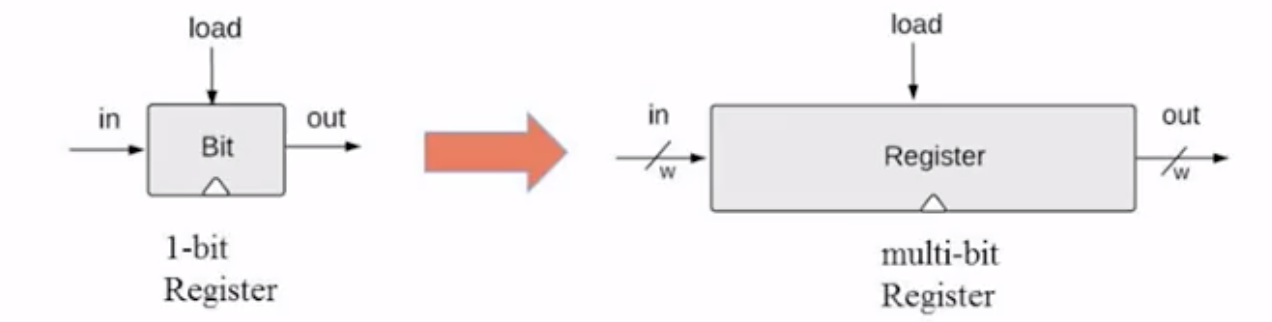
- We use 16-bit word width to keep generality
- “Word width” is a parameter
w, which can be 32-bit, 64-bit, too.
Register’s State: the value which is currently stored in the register.
Read Logic
This is easy, just probe the out and see the outputs.
Write Logic
Say, we want the register to remember the number 123. We can:
- set
in = 123 - set
load = 1 - The
outwill emit123from the next time unit.
How in the Hardware Simulator?
- Load in the HDL file
nand2tetris\tools\builtInChips\DRegister.hdl. - See the key word
BUILTINandCLOCKED. This chip is actually implemented by a Java class. When the key wordCLOCKEDis detected, the clock-shaped button will be activated. - The “Time: __” will tick to “0+” and then tock to “1”. The GUI “D: “ on the right displays the value of DFF (defaulted “0”). However, the output pin takes a complete cycle to emit the newly loaded value.
RAM Unit
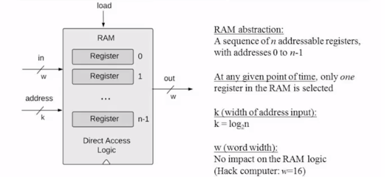
- Abstractly, we view RAM unit as a sequence of $n$ addressable registers, with address
0ton - 1. - At any point of time, only one register can be selected no matter how many registers exist.
- To represent the address input, it should be $k$ long, where $k = \log_2 n$.
- $n$ has nothing to do with the word width $w$.
- In a word, RAM is a sequential chip, and it depends on a clock input.
Read & Write Logic
The same as a single register, except switching the address code.
A family of 16-bit RAM chips
The family has the same generic architecture as showed above.
As the number of registers, $n$, goes up, the chips are RAM8, RAM64, RAM32, RAM4K, RAM16K… Accordingly, $k$ is respectively 3, 6, 9, 12, 14…
Why these 5 particular RAM chips?
Stay tuned… we need them for the next Hack Computer.
Why “Random Access”?
RAM stands for “Random Access Memory”, because a magic thing is, once the address code is provide, no matter how many registers, 8 or 8 million, the data is accessible after the same moment.
Counter
The computer needs a Program Counter (PC) to keep track of the instruction which should be fetched and executed next.
The PC contains the address of the instruction to fetch.
3 control settings:
- Reset: fetch the first instruction
pc = 0 - Next: fetch the next instruction
pc++ - Goto: fetch instruction
npc = n
Inputs & Outputs
1 | IN in[16], laod, inc, reset; |
Chip Logic
1 | if (reset[t] == 1) |
How in the Hardware Simulator?
- Load in the HDL file
nand2tetris\tools\builtInChips\PC.hdl. - Note the priority:
resetfirst, thenload,incat last. - The
>>button can tick the clock automatically every second.